- 您现在的位置:买卖IC网 > Sheet目录1995 > HI1175JCB-T (Intersil)CONV A/D 8BIT 20MSPS 24-SOIC
3
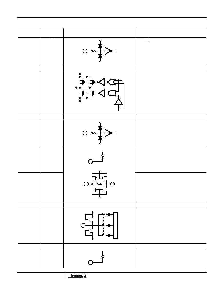
Pin Descriptions and Equivalent Circuits
PIN
NUMBER
SYMBOL
EQUIVALENT CIRCUIT
DESCRIPTION
1OE
When OE = Low, Data is valid.
When OE = High, D0 to D7 pins high impedance.
2, 24
DVSS
Digital GND.
3-10
D0 to D7
D0 (LSB) to D7 (MSB) Output.
11, 13
DVDD
Digital +5V.
12
CLK
Clock Input.
16
VRTS
Shorted with VRT generates, +2.6V.
17
VRT
Reference Voltage (Top).
23
VRB
Reference Voltage (Bottom).
14, 15, 18
AVDD
Analog +5V.
19
VIN
Analog Input.
20, 21
AVSS
Analog GND.
22
VRBS
Shorted with VRB generates +0.6V.
1
DVDD
DVSS
D1
12
DVDD
DVSS
16
AVDD
AVSS
17
23
AVDD
AVSS
19
22
AVSS
HI1175
发布紧急采购,3分钟左右您将得到回复。
相关PDF资料
HI1178JCQ
CONV D/A 8BIT TRPL 40MHZ 48-PQFP
HI3-674AKN-5
IC ADC 12BIT 67KSPS 28-SBDIP
HI3-7159A-5Z
IC ADC 5-1/2 DIGIT 28-PDIP
HI3-DAC80V-5
CONV D/A 12BIT OUTPUT AMP 24PDIP
HI3026JCQ
ADC FLASH 8BIT 120MSPS 48-PQFP
HI3338KIBZ
IC DAC 8BIT CMOS 16-SOIC
HI5628INZ
IC DAC 8BIT 125MSPS DUAL 48-LQFP
HI5660IBZ
CONV D/A 8-BIT 125MSPS 28-SOIC
相关代理商/技术参数
HI1175JCP
制造商:Harris Corporation 功能描述:
HI1176
制造商:INTERSIL 制造商全称:Intersil Corporation 功能描述:8-Bit, 20 MSPS, Flash A/D Converter
HI1176_05
制造商:INTERSIL 制造商全称:Intersil Corporation 功能描述:8-Bit, 20 MSPS, Flash A/D Converter
HI1176-EV
制造商:INTERSIL 制造商全称:Intersil Corporation 功能描述:8-Bit, 20 MSPS, Flash A/D Converter
HI1176JCQ
制造商:Rochester Electronics LLC 功能描述:32 PQFP INDTEMP VIDEO A/D 8 BIT 20MSPS SYNC-CLAMP V-REF - Bulk
HI1176JCQ-T
制造商:Rochester Electronics LLC 功能描述:- Bulk
HI1177
制造商:INTERSIL 制造商全称:Intersil Corporation 功能描述:8-Bit, 40MSPS, 2-Channel D/A Converter
HI1177JCQ
制造商:Rochester Electronics LLC 功能描述:32 PQFP INDTEMP DUAL VIDEO D/A 8BIT 40MHZ - Bulk 制造商:Harris Corporation 功能描述: